


Laser-Cut vs. Etched vs. Electroformed: Choosing the Right PCB Stencil 🛠️
 View
View
If you're still hand-soldering SMD components pad-by-pad, you're playing life on "Hard Mode". Switching to a PCB Stencil and solder paste is the single biggest upgrade you can make for your workflow—but not all stencils are created equal.
Depending on your pitch size and budget, the manufacturing process matters. Here's the breakdown:
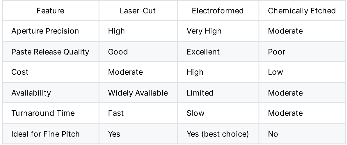
Chemical Etched Stencils (The "Old School" Choice)
These are made by using a chemical etchant to eat through the metal.
- The Catch: The etching solution doesn't just go down; it goes sideways. This creates "undercutting," resulting in a slightly trapezoidal opening.
- Best for: Large components and hobbyist projects where ultra-precision isn't a dealbreaker.
Laser-Cut Stencils (The Industry Standard)
This is the "sweet spot" for 99% of us. A CNC laser cuts the apertures with incredible accuracy.
- The Perk: The laser naturally creates a slight inward taper. This actually helps the solder paste release cleanly from the stencil onto your board.
- Best for: Most modern SMD designs, including QFNs and 0402s.
Electroformed Stencils (The Pro Tier)
These aren't "cut"—they are "grown" atom-by-atom through nickel plating.
- The Perk: The walls are atom-level smooth. If you are dealing with ultra-fine pitch BGAs or 0201 components, this is the only way to ensure 100% consistent paste release.
- Best for: High-density, professional-grade production.
🚀 Level Up Your Assembly
Ready to ditch the soldering iron and start stenciling? We've got you covered at JLCPCB.
- 🎁 Click to claim an $11 Stencil Coupon now!
- ✨ New to JLCPCB? Register now and grab a $123 New User Coupon Bundle to kickstart your next project.
SMT Stencil
Sign In Or Register Comment after
No comments yet. Be the first to comment!